SFP-1.25G-1310nm-20km-SM-LC-DDM
1.25Gb/s 1310nm Single-mode SFP Transceiver
PRODUCT FEATURES
● Up to 1.25Gb/s data links
● FP laser transmitter and PIN photo-detector
● Up to 20km on 9/125µm SMF
● Hot-pluggable SFP footprint
● Duplex LC/UPC type pluggable optical interface
● Low power dissipation
● Metal enclosure, for lower EMI
● RoHS compliant and lead-free
● Single +3.3V power supply
● Compliant with SFF-8472
● Case operating temperature
Commercial: 0°C to +70°C
Extended: -10°C to +80°C
Industrial: -40°C to +85°C
APPLICATIONS
● Switch to Switch Interface
● Gigabit Ethernet
● Switched Backplane Applications
● Router/Server Interface
● Other Optical Links

PRODUCT DESCRIPTION
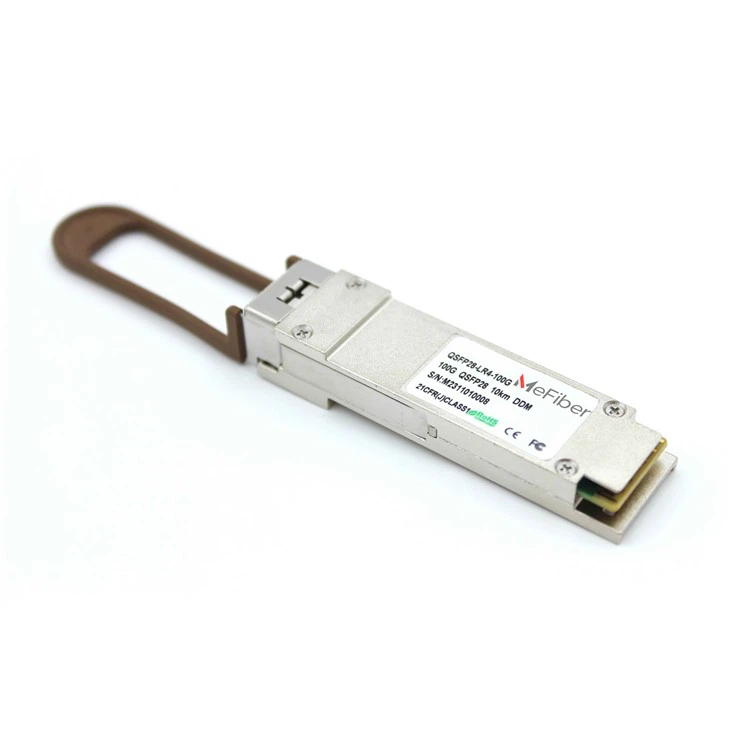
SFP-1.25G-1310nm-20km-SM-LC-DDM Small Form Factor Pluggable (SFP) transceivers are compatible with the Small Form Factor Pluggable Multi-Sourcing Agreement (MSA). The transceiver consists of four sections: the LD driver, the limiting amplifier, the FP laser and the PIN photo-detector .The module data link up to 20km in 9/125um single mode fiber.
Ordering information
|
Product part Number |
Data Rate (Mbps) |
Media |
Wavelength (nm) |
Transmission Distance(km) |
Temperature Range(Tcase)(℃) |
|
|
SFP-1.25G-1310nm-20km-SM-LC-DDM |
1250 |
Single mode fiber |
1310 |
20 |
0~70 |
commercial |
|
SFP-1.25G-1310nm-20km-SM-LC-DDM |
1250 |
Single mode fiber |
1310 |
20 |
-10~80 |
extended |
|
SFP-1.25G-1310nm-20km-SM-LC-DDM |
1250 |
Single mode fiber |
1310 |
20 |
-40~85 |
industrial |
I. Pin Descriptions
|
Pin |
Symbol |
Name/Description |
NOTE |
|
1 |
VEET |
Transmitter Ground (Common with Receiver Ground) |
1 |
|
2 |
TFAULT |
Transmitter Fault. |
|
|
3 |
TDIS |
Transmitter Disable. Laser output disabled on high or open. |
2 |
|
4 |
MOD_DEF(2) |
Module Definition 2. Data line for Serial ID. |
3 |
|
5 |
MOD_DEF(1) |
Module Definition 1. Clock line for Serial ID. |
3 |
|
6 |
MOD_DEF(0) |
Module Definition 0. Grounded within the module. |
3 |
|
7 |
Rate Select |
No connection required |
4 |
|
8 |
LOS |
Loss of Signal indication. Logic 0 indicates normal operation. |
5 |
|
9 |
VEER |
Receiver Ground (Common with Transmitter Ground) |
1 |
|
10 |
VEER |
Receiver Ground (Common with Transmitter Ground) |
1 |
|
11 |
VEER |
Receiver Ground (Common with Transmitter Ground) |
1 |
|
12 |
RD- |
Receiver Inverted DATA out. AC Coupled |
|
|
13 |
RD+ |
Receiver Non-inverted DATA out. AC Coupled |
|
|
14 |
VEER |
Receiver Ground (Common with Transmitter Ground) |
1 |
|
15 |
VCCR |
Receiver Power Supply |
|
|
16 |
VCCT |
Transmitter Power Supply |
|
|
17 |
VEET |
Transmitter Ground (Common with Receiver Ground) |
1 |
|
18 |
TD+ |
Transmitter Non-Inverted DATA in. AC Coupled. |
|
|
19 |
TD- |
Transmitter Inverted DATA in. AC Coupled. |
|
|
20 |
VEET |
Transmitter Ground (Common with Receiver Ground) |
1 |
Notes:
1. Circuit ground is internally isolated from chassis ground.
2. Laser output disabled on TDIS >2.0V or open, enabled on TDIS <0.8V.
3. Should be pulled up with 4.7k - 10kohms on host board to a voltage between 2.0V and 3.6V.MOD_DEF (0) pulls line low to indicate module is plugged in.
4. This is an optional input used to control the receiver bandwidth for compatibility with multiple data rates (most likely Fiber Channel 1x and 2x Rates).If implemented, the input will be internally pulled down with > 30kΩ resistor. The input states are:
◆ Low (0 – 0.8V): Reduced Bandwidth
◆ (>0.8, < 2.0V): Undefined
◆ High (2.0 – 3.465V): Full Bandwidth
◆ Open: Reduced Bandwidth
5. LOS is open collector output should be pulled up with 4.7k - 10kohms on host board to a voltage between 2.0V and 3.6V. Logic 0 indicates normal operation; logic 1 indicates loss of signal.

Figure2. Pin out of Connector Block on Host Board
II. Absolute Maximum Ratings
|
Parameter |
Symbol |
Min. |
Typ. |
Max. |
Unit |
Note |
|
Storage Temperature |
Ts |
-40 |
85 |
ºC |
||
|
Relative Humidity |
RH |
5 |
95 |
% |
||
|
Power Supply Voltage |
VCC |
-0.5 |
4 |
V |
||
|
Signal Input Voltage |
-0.3 |
Vcc+0.3 |
V |
|||
|
Receiver Damage Threshold |
+5 |
dBm |
III. Recommended Operating Conditions
|
Parameter |
Symbol |
Min. |
Typ. |
Max. |
Unit |
Note |
|
Case Operating Temperature |
Tcase |
0 |
70 |
ºC |
SFP-1.25G-1310nm-20km-SM-LC-DDM |
|
|
-10 |
80 |
SFP-1.25G-1310nm-20km-SM-LC-DDM |
||||
|
-40 |
85 |
SFP-1.25G-1310nm-20km-SM-LC-DDM |
||||
|
Power Supply Voltage |
VCC |
3.13 |
3.3 |
3.47 |
V |
|
|
Power Supply Current |
ICC |
280 |
mA |
|||
|
Power Supply Noise Rejection |
100 |
mVp-p |
100Hz to 1MHz |
|||
|
Data Rate |
1250/1250 |
Mbps |
TX Rate/RX Rate |
|||
|
Transmission Distance |
20 |
KM |
||||
|
Coupled Fiber |
Single mode fiber |
9/125um SMF |
||||
IV. Specification of Transmitter
|
Parameter |
Symbol |
Min. |
Typ. |
Max. |
Unit |
Note |
|
Case Operating Temperature |
Tcase |
0 |
70 |
ºC |
SFP-1.25G-1310nm-20km-SM-LC-DDM |
|
|
-10 |
80 |
SFP-1.25G-1310nm-20km-SM-LC-DDM |
||||
|
-40 |
85 |
SFP-1.25G-1310nm-20km-SM-LC-DDM |
||||
|
Power Supply Voltage |
VCC |
3.13 |
3.3 |
3.47 |
V |
|
|
Power Supply Current |
ICC |
280 |
mA |
|||
|
Power Supply Noise Rejection |
100 |
mVp-p |
100Hz to 1MHz |
|||
|
Data Rate |
1250/1250 |
Mbps |
TX Rate/RX Rate |
|||
|
Transmission Distance |
20 |
KM |
||||
|
Coupled Fiber |
Single mode fiber |
9/125um SMF |
||||
Note (1): Measure at 2^7-1 NRZ PRBS pattern
Note (2): Transmitter eye mask definition

V. Specification of Receiver
|
Parameter |
Symbol |
Min. |
Typ. |
Max. |
Unit |
Note |
|
Input Optical Wavelength |
λIN |
1270 |
1610 |
nm |
PIN-TIA |
|
|
Receiver Sensitivity |
PIN |
-20 |
dBm |
Note (1) |
||
|
Input Saturation Power (Overload) |
PSAT |
-3 |
dBm |
|||
|
Los Of Signal Assert |
PA |
-22 |
dBm |
|||
|
Los Of Signal De-assert |
PD |
-35 |
dBm |
Note (2) |
||
|
LOS Hysteresis |
PA-PD |
0.5 |
2 |
6 |
dB |
Note (1): Measured with Light source 1310nm, ER=9dB; BER =<10^-12 @PRBS=2^7-1 NRZ
Note (2): When SD De-Assert, the RX-LOS output is High-level (fixed)
VI. Electrical Interface Characteristics
|
Parameter |
Symbol |
Min. |
Typ. |
Max. |
Unit |
Note |
|
Transmitter |
||||||
|
Total Supply Current |
ICC |
A |
mA |
Note (1) |
||
|
Transmitter Disable Input-High |
VDISH |
2 |
Vcc+0.3 |
V |
||
|
Transmitter Disable Input-Low |
VDISL |
0 |
0.8 |
V |
||
|
Transmitter Fault Input-High |
VTxFH |
2 |
Vcc+0.3 |
V |
||
|
Transmitter Fault Input-Low |
VTxFL |
0 |
0.8 |
V |
||
|
Receiver |
||||||
|
Total Supply Current |
ICC |
B |
mA |
Note (1) |
||
|
LOSS Output Voltage-High |
VLOSH |
2 |
Vcc+0.3 |
V |
LVTTL |
|
|
LOSS Output Voltage-Low |
VLOSL |
0 |
0.8 |
V |
||
Note (1): A (TX) + B (RX) = 280mA (Not include termination circuit)
VII. Mechanical Specifications

SFP-1.25G-1310nm-20km-SM-LC-DDM
VIII.Regulatory Compliance
|
Feature |
Reference |
Performance |
|
Electrostatic discharge(ESD) |
IEC/EN 61000-4-2 |
Compatible with standards |
|
Electromagnetic Interference (EMI) |
FCC Part 15 Class B EN 55022 Class B (CISPR 22A) |
Compatible with standards |
|
Laser Eye Safety |
FDA 21CFR 1040.10, 1040.11 IEC/EN 60825-1,2 |
Class 1 laser product |
|
Component Recognition |
IEC/EN 60950 ,UL |
Compatible with standards |
|
ROHS |
2002/95/EC |
Compatible with standards |
|
EMC |
EN61000-3 |
Compatible with standards |
Appendix A. Document Revision
|
Version No. |
Date |
Description |
|
1.0 |
2021.7.22 |
Preliminary datasheet |